 W
WAngel gilding is gilding glass or gold plating by electroless chemical deposition.
 W
WChemical vapor deposition (CVD) is a vacuum deposition method used to produce high quality, and high-performance, solid materials. The process is often used in the semiconductor industry to produce thin films.
 W
WClosed space sublimation is a method of producing thin-films, esp. cadmium telluride photovoltaics, though it is used for other materials like antimony triselenide.
 W
WDiamond-like carbon (DLC) is a class of amorphous carbon material that displays some of the typical properties of diamond. DLC is usually applied as coatings to other materials that could benefit from such properties.
 W
WDip coating is an industrial coating process which is used, for example, to manufacture bulk products such as coated fabrics and condoms and specialised coatings for example in the biomedical field. Dip coating is also commonly used in academic research, where many chemical and nano material engineering research projects use the dip coating technique to create thin-film coatings.
 W
WEpitaxy refers to a type of crystal growth or material deposition in which new crystalline layers are formed with one or more well-defined orientations with respect to the crystalline seed layer. The deposited crystalline film is called an epitaxial film or epitaxial layer. The relative orientation(s) of the epitaxial layer to the seed layer is defined in terms of the orientation of the crystal lattice of each material. For most epitaxial growths, the new layer is usually crystalline and each crystallographic domain of the overlayer must have a well-defined orientation relative to the substrate crystal structure. Epitaxy can involve single-crystal structures, although grain-to-grain epitaxy has been observed in granular films. For most technological applications, single domain epitaxy, which is the growth of an overlayer crystal with one well-defined orientation with respect to the substrate crystal, is preferred. Epitaxy can also play an important role while growing superlattice structures.
 W
WEvaporation is a type of vaporization that occurs on the surface of a liquid as it changes into the gas phase. The surrounding gas must not be saturated with the evaporating substance. When the molecules of the liquid collide, they transfer energy to each other based on how they collide with each other. When a molecule near the surface absorbs enough energy to overcome the vapor pressure, it will escape and enter the surrounding air as a gas. When evaporation occurs, the energy removed from the vaporized liquid will reduce the temperature of the liquid, resulting in evaporative cooling.
 W
WEvaporation is a common method of thin-film deposition. The source material is evaporated in a vacuum. The vacuum allows vapor particles to travel directly to the target object (substrate), where they condense back to a solid state. Evaporation is used in microfabrication, and to make macro-scale products such as metallized plastic film.
 W
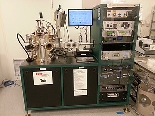
WFocused ion beam, also known as FIB, is a technique used particularly in the semiconductor industry, materials science and increasingly in the biological field for site-specific analysis, deposition, and ablation of materials. A FIB setup is a scientific instrument that resembles a scanning electron microscope (SEM). However, while the SEM uses a focused beam of electrons to image the sample in the chamber, a FIB setup uses a focused beam of ions instead. FIB can also be incorporated in a system with both electron and ion beam columns, allowing the same feature to be investigated using either of the beams. FIB should not be confused with using a beam of focused ions for direct write lithography. These are generally quite different systems where the material is modified by other mechanisms.
 W
WHybrid physical–chemical vapor deposition (HPCVD) is a thin-film deposition technique, that combines physical vapor deposition (PVD) with chemical vapor deposition (CVD).
 W
WAn ion beam is a type of charged particle beam consisting of ions. Ion beams have many uses in electronics manufacturing and other industries. A variety of ion beam sources exists, some derived from the mercury vapor thrusters developed by NASA in the 1960s. The most common ion beams are of singly-charged ions.
 W
WIon beam deposition (IBD) is a process of applying materials to a target through the application of an ion beam.
 W
WIon layer gas reaction (ILGAR®) is a non-vacuum, thin-film deposition technique developed and patented by the group of Professor Dr. Christian-Herbert Fischer at the Helmholtz-Zentrum Berlin for materials and energy in Berlin, Germany. It is a sequential and cyclic process that enables the deposition of semiconductor thin films, mainly for photovoltaic applications, specially chalcopyrite absorber layers and buffer layers. The ILGAR technique was awarded as German High Tech Champion 2011 by the Fraunhofer Society.
 W
WIon plating (IP) is a physical vapor deposition (PVD) process that is sometimes called ion assisted deposition (IAD) or ion vapor deposition (IVD) and is a version of vacuum deposition. Ion plating uses concurrent or periodic bombardment of the substrate, and deposits film by atomic-sized energetic particles. Bombardment prior to deposition is used to sputter clean the substrate surface. During deposition the bombardment is used to modify and control the properties of the depositing film. It is important that the bombardment be continuous between the cleaning and the deposition portions of the process to maintain an atomically clean interface.
 W
WThe Lely method, also known as the Lely process or Lely technique, is a crystal growth technology used for producing silicon carbide crystals for the semiconductor industry. The patent for this method was filed in the Netherlands in 1954 and in the United States in 1955 by Jan Anthony Lely of Philips Electronics. The patent was subsequently granted on 30 September 1958, and was refined by D.R. Hamilton et al. in 1960, and by V.P. Novikov and V.I. Ionov in 1968.
 W
WLow-energy plasma-enhanced chemical vapor deposition (LEPECVD) is a plasma-enhanced chemical vapor deposition technique used for the epitaxial deposition of thin semiconductor films. A remote low energy, high density DC argon plasma is employed to efficiently decompose the gas phase precursors while leaving the epitaxial layer undamaged, resulting in high quality epilayers and high deposition rates.
 W
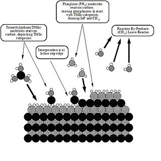
WMetalorganic vapour-phase epitaxy (MOVPE), also known as organometallic vapour-phase epitaxy (OMVPE) or metalorganic chemical vapour deposition (MOCVD), is a chemical vapour deposition method used to produce single- or polycrystalline thin films. It is a process for growing crystalline layers to create complex semiconductor multilayer structures. In contrast to molecular-beam epitaxy (MBE), the growth of crystals is by chemical reaction and not physical deposition. This takes place not in vacuum, but from the gas phase at moderate pressures. As such, this technique is preferred for the formation of devices incorporating thermodynamically metastable alloys, and it has become a major process in the manufacture of optoelectronics, such as Light-emitting diodes. It was invented in 1968 at North American Aviation Science Center by Harold M. Manasevit.
 W
WMolecular-beam epitaxy (MBE) is an epitaxy method for thin-film deposition of single crystals. MBE is widely used in the manufacture of semiconductor devices, including transistors, and it is considered one of the fundamental tools for the development of nanotechnologies. MBE is used to fabricate diodes and MOSFETs at microwave frequencies, and to manufacture the lasers used to read optical discs.
 W
WPhysical vapor deposition (PVD), sometimes called physical vapor transport (PVT), describes a variety of vacuum deposition methods which can be used to produce thin films and coatings. PVD is characterized by a process in which the material goes from a condensed phase to a vapor phase and then back to a thin film condensed phase. The most common PVD processes are sputtering and evaporation. PVD is used in the manufacture of items which require thin films for mechanical, optical, chemical or electronic functions. Examples include semiconductor devices such as thin film solar panels, aluminized PET film for food packaging and balloons, and titanium nitride coated cutting tools for metalworking. Besides PVD tools for fabrication, special smaller tools have been developed.
 W
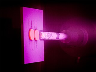
WPlasma-enhanced chemical vapor deposition (PECVD) is a chemical vapor deposition process used to deposit thin films from a gas state (vapor) to a solid state on a substrate. Chemical reactions are involved in the process, which occur after creation of a plasma of the reacting gases. The plasma is generally created by radio frequency (RF) frequency or direct current (DC) discharge between two electrodes, the space between which is filled with the reacting gases.
 W
WPulsed laser deposition (PLD) is a physical vapor deposition (PVD) technique where a high-power pulsed laser beam is focused inside a vacuum chamber to strike a target of the material that is to be deposited. This material is vaporized from the target which deposits it as a thin film on a substrate. This process can occur in ultra high vacuum or in the presence of a background gas, such as oxygen which is commonly used when depositing oxides to fully oxygenate the deposited films.
 W
WSpin coating is a procedure used to deposit uniform thin films onto flat substrates. Usually a small amount of coating material is applied on the center of the substrate, which is either spinning at low speed or not spinning at all. The substrate is then rotated at speed up to 10,000 rpm to spread the coating material by centrifugal force. A machine used for spin coating is called a spin coater, or simply spinner.
 W
WSputter deposition is a physical vapor deposition (PVD) method of thin film deposition by sputtering. This involves ejecting material from a "target" that is a source onto a "substrate" such as a silicon wafer. Resputtering is re-emission of the deposited material during the deposition process by ion or atom bombardment. Sputtered atoms ejected from the target have a wide energy distribution, typically up to tens of eV. The sputtered ions can ballistically fly from the target in straight lines and impact energetically on the substrates or vacuum chamber. Alternatively, at higher gas pressures, the ions collide with the gas atoms that act as a moderator and move diffusively, reaching the substrates or vacuum chamber wall and condensing after undergoing a random walk. The entire range from high-energy ballistic impact to low-energy thermalized motion is accessible by changing the background gas pressure. The sputtering gas is often an inert gas such as argon. For efficient momentum transfer, the atomic weight of the sputtering gas should be close to the atomic weight of the target, so for sputtering light elements neon is preferable, while for heavy elements krypton or xenon are used. Reactive gases can also be used to sputter compounds. The compound can be formed on the target surface, in-flight or on the substrate depending on the process parameters. The availability of many parameters that control sputter deposition make it a complex process, but also allow experts a large degree of control over the growth and microstructure of the film.
 W
WIn physics, sputtering is a phenomenon in which microscopic particles of a solid material are ejected from its surface, after the material is itself bombarded by energetic particles of a plasma or gas. It occurs naturally in outer space, and can be an unwelcome source of wear in precision components. However, the fact that it can be made to act on extremely fine layers of material is utilised in science and industry—there, it is used to perform precise etching, carry out analytical techniques, and deposit thin film layers in the manufacture of optical coatings, semiconductor devices and nanotechnology products. It is a physical vapor deposition technique.
WThe sublimation sandwich method is a kind of physical vapor deposition used for creating man-made crystals. Silicon carbide is the most common crystal grown this way, though others crystals may also be created with it.
 W
WThermal barrier coatings (TBCs) are advanced materials systems usually applied to metallic surfaces operating at elevated temperatures, such as gas turbine or aero-engine parts, as a form of exhaust heat management. These 100 μm to 2 mm thick coatings of thermally insulating materials serve to insulate components from large and prolonged heat loads and can sustain an appreciable temperature difference between the load-bearing alloys and the coating surface. In doing so, these coatings can allow for higher operating temperatures while limiting the thermal exposure of structural components, extending part life by reducing oxidation and thermal fatigue. In conjunction with active film cooling, TBCs permit working fluid temperatures higher than the melting point of the metal airfoil in some turbine applications. Due to increasing demand for more efficient engines running at higher temperatures with better durability/lifetime and thinner coatings to reduce parasitic mass for rotating/moving components, there is significant motivation to develop new and advanced TBCs. The material requirements of TBCs are similar to those of heat shields, although in the latter application emissivity tends to be of greater importance.
 W
WThermal spraying techniques are coating processes in which melted materials are sprayed onto a surface. The "feedstock" is heated by electrical or chemical means.
 W
WTinning is the process of thinly coating sheets of wrought iron or steel with tin, and the resulting product is known as tinplate. The term is also widely used for the different process of coating a metal with solder before soldering.
 W
WVacuum deposition is a group of processes used to deposit layers of material atom-by-atom or molecule-by-molecule on a solid surface. These processes operate at pressures well below atmospheric pressure. The deposited layers can range from a thickness of one atom up to millimeters, forming freestanding structures. Multiple layers of different materials can be used, for example to form optical coatings. The process can be qualified based on the vapor source; physical vapor deposition uses a liquid or solid source and chemical vapor deposition uses a chemical vapor.
 W
WVacuum evaporation is the process of causing the pressure in a liquid-filled container to be reduced below the vapor pressure of the liquid, causing the liquid to evaporate at a lower temperature than normal. Although the process can be applied to any type of liquid at any vapor pressure, it is generally used to describe the boiling of water by lowering the container's internal pressure below standard atmospheric pressure and causing the water to boil at room temperature.
 W
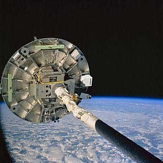
WWake Shield Facility (WSF) was an experimental science platform that was placed in low Earth orbit by the Space Shuttle. It was a 3.7 meters (12 ft) diameter, free-flying stainless steel disk.