 W
WCo-fired ceramic devices are monolithic, ceramic microelectronic devices where the entire ceramic support structure and any conductive, resistive, and dielectric materials are fired in a kiln at the same time. Typical devices include capacitors, inductors, resistors, transformers, and hybrid circuits. The technology is also used for robust assembly and packaging of electronic components multi-layer packaging in the electronics industry, such as military electronics, MEMS, microprocessor and RF applications.
 W
WCompliant bonding is used to connect gold wires to electrical components such as integrated circuit "chips". It was invented by Alexander Coucoulas in the 1960s. The bond is formed well below the melting point of the mating gold surfaces and is therefore referred to as a solid-state type bond. The compliant bond is formed by transmitting heat and pressure to the bond region through a relatively thick indentable or compliant medium, generally an aluminum tape.
 W
WAlexander Coucoulas is an American inventor, research engineer, and author. He was named "Father Of Thermosonic Bonding" by George Harman, the world's foremost authority on wire bonding, where he referenced Coucoulas's leading edge publications in his book, Wire Bonding In Microelectronics. A Thermosonic bond is formed using a set of parameters which include ultrasonic, thermal and mechanical (force) energies. Figure 1 (below) shows a diagram of a Thermosonic Bonding machine which includes a magnetostrictive or piezoelectric-type transducer which is used to convert electrical energy into vibratory motion. The vibratory motion travels along the coupler system, a portion which is tapered to serve as the velocity transformer. The velocity transformer amplifies the oscilliatory motion and delivers it to a heated bonding tip.
 W
WEutectic bonding, also referred to as eutectic soldering, describes a wafer bonding technique with an intermediate metal layer that can produce a eutectic system. Those eutectic metals are alloys that transform directly from solid to liquid state, or vice versa from liquid to solid state, at a specific composition and temperature without passing a two-phase equilibrium, i.e. liquid and solid state. The fact that the eutectic temperature can be much lower than the melting temperature of the two or more pure elements can be important in eutectic bonding.
 W
WIn electronics manufacturing, integrated circuit packaging is the final stage of semiconductor device fabrication, in which the block of semiconductor material is encapsulated in a supporting case that prevents physical damage and corrosion. The case, known as a "package", supports the electrical contacts which connect the device to a circuit board.
 W
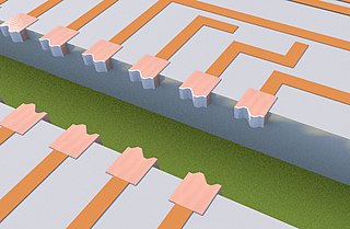
WQuilt Packaging (QP) is an integrated circuit packaging and chip-to-chip interconnect packaging technology that utilizes “nodule” structures that extend out horizontally from the edges of microchips to make electrically and mechanically robust chip-to-chip interconnections.
 W
WIn integrated circuit packaging, a solder ball, also a solder bump is a ball of solder that provides the contact between the chip package and the printed circuit board, as well as between stacked packages in multichip modules; in the latter case, they may be referred to as microbumps, since they are usually significantly smaller than the former. The solder balls can be placed manually or by automated equipment, and are held in place with a tacky flux.
 W
WA system in a package (SiP) or system-in-package is a number of integrated circuits enclosed in one or more chip carrier packages that may be stacked using package on package. The SiP performs all or most of the functions of an electronic system, and is typically used inside a mobile phone, digital music player, etc. Dies containing integrated circuits may be stacked vertically on a substrate. They are internally connected by fine wires that are bonded to the package. Alternatively, with a flip chip technology, solder bumps are used to join stacked chips together. A SiP is like a system on a chip (SoC) but less tightly integrated and not on a single semiconductor die.
 W
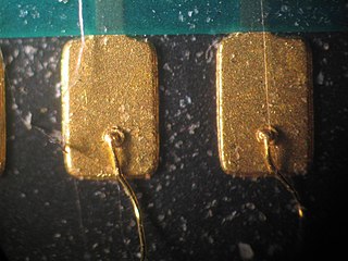
WWire bonding is the method of making interconnections between an integrated circuit (IC) or other semiconductor device and its packaging during semiconductor device fabrication. Although less common, wire bonding can be used to connect an IC to other electronics or to connect from one printed circuit board (PCB) to another. Wire bonding is generally considered the most cost-effective and flexible interconnect technology and is used to assemble the vast majority of semiconductor packages. Wire bonding can be used at frequencies above 100 GHz.